Germany Section Solid-State Circuits Society Chapter
Upcoming events
- Future technical meetings of the German Chapter of the IEEE Solid-State Circuits’ Society will be announced here.
-
Introduction to Electronics for Quantum Applications and the Cluster4Future QSens
Date and Time
- Date: 29. June2025
- Time: 05:00 PM to 06:30 PM
- All times are (UTC+01:00) Berlin
Location
- Virtual attendance.
Hosts
Registration
-
- Starts 20. June 2025 12:00 AM
- Ends 29. June 2025 04:00 PM
- All times are (UTC+01:00) Berlin
- No Admission Charge
- https://events.vtools.ieee.org/m/489834
Speaker
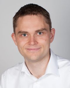
- Prof. Dr. Jens Anders, Stuttgart University
Description
The talk “Introduction to Electronics for Quantum Applications and the Cluster4Future QSens” will present an overview of the critical role of interface electronics in enabling practical quantum technologies, with a particular focus on quantum sensing applications. As quantum sensors exploit phenomena such as superposition and entanglement to achieve unprecedented sensitivity and resolution, their performance heavily depends on the design and integration of dedicated electronic systems for signal generation, readout, and control.
The first part of the lecture will provide an introduction to the unique requirements of interface electronics for quantum sensors. This includes low-noise analog front-ends, high-precision timing and synchronization, and dedicated RF transceiver circuits. Practical challenges and current solutions in interfacing quantum systems with classical electronics will be discussed, highlighting the importance of co-design across physical, electronic, and algorithmic layers.
While the primary focus is on quantum sensing, the talk will also briefly touch upon electronics for quantum computing, particularly in terms of scalable control and readout of qubits. Key differences and overlaps between the electronic needs of sensing and computing applications will be outlined.
The second part of the presentation will introduce the Cluster4Future QSens, a German research and innovation initiative aimed at accelerating the development and commercialization of quantum sensing technologies. The cluster’s goals, structure, and research activities will be presented, with selected project examples showcasing collaborative efforts between academic institutions and industry partners.
This talk is aimed at students, researchers, and professionals interested in the intersection of quantum technologies and electronic system design, offering insights into current developments and future directions in the field.
Speaker Biography

- Jens Anders (Senior Member, IEEE) received the M.Sc. degree from the University of Michigan, Ann Arbor, MI, USA, in 2005, the Dipl.-Ing. degree from Leibniz University Hannover, Hanover, Germany, in 2007, and the Ph.D. degree from the École Polytechnique Fédérale de Lausanne, Lausanne, Switzerland, in 2011. From 2013 to 2017, he was an Assistant Professor with the Institute of Microelectronics, University of Ulm, Ulm, Germany. Currently, he is a Full Professor and the Director of the Institute of Smart Sensors at the University of Stuttgart, Stuttgart, Germany. Since 2022, he has also been the Co-Director of the Institute for Microelectronics Stuttgart (IMS CHIPS), Stuttgart. He has authored or co-authored several books and book chapters, and more than 200 journal and conference papers. His research interests include circuit design for sensing applications, including materials science and biomedical, and quantum sensing. He was a member of the Program Committee for ESSCIRC, ESSDERC, ESSERC, IEEE SENSORS, and ISSCC. He was the recipient of the 2015 ITG Publication Award, the Best Live Demo Award at the 2017 IEEE SENSORS, the 2019 Helmholtz Center Berlin Technology Transfer Award, and one of the 2020 Sony Europe Research Awards. He was an Associate Editor for IEEE TRANSACTIONS ON CIRCUITS AND SYSTEMS-II: EXPRESS BRIEFS and a Guest Editor of IEEE JOURNAL OF SOLID-STATE CIRCUITS and IEEE SOLID-STATE CIRCUITS LETTERS.
Recent past events
-
BIO-IMPLANTABLE INTEGRATED CIRCUITS: OPPORTUNITIES, CHALLENGES AND THE FUTURE
Date and Time
- Date: 23 Jun 2024
- Time: 06:00 PM to 07:30 PM
- All times are (UTC+02:00) Berlin
Location
- Virtual attendance.
Hosts
- Germany Section Chapter, SSC37
- Germany Section Chapter, CAS04
- Egypt Section Chapter, SSC37
Registration
- Starts 02 June 2024 12:00 AM
- Ends 23 June 2024 12:00 AM
- All times are (UTC+02:00) Berlin
- No Admission Charge
Speaker
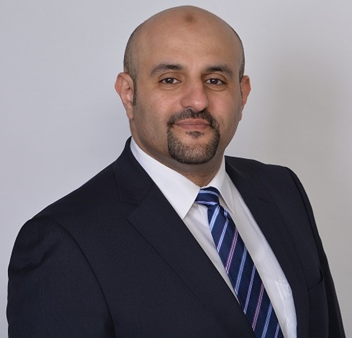
- Prof. Dr.-Ing. Moustafa Nawito of IU Internationale Hochschule / Polymath Analog
Motivation
Implantable electronics play an essential role in the Advancement of medical devices. The introduction of the pacemaker in 1958 ushered in the era of active implants. Since then, numerous applications have benefited from Implantable electronics, such as cochlear implants and Nerve stimulators. With the advent of integrated circuits and new Manufacturing technologies, implantable electronics have Been used in new areas outside the healthcare industry. Over the years, a wealth of knowledge has accumulated in which specialized design techniques and circuits have been developed to meet the needs of implantable applications.
Aim
This Talk offers a comprehensive overview on the topic of implantable electronics. A primary focus is on presenting the special requirements and specifications of implantable electronics that arise from their respective applications, as well as an overview of the various techniques and methods used to meet these requirements. The electronic components of several implantable devices are presented, in addition to the corresponding manufacturing processes. Discussion of the technical aspects of implantable electronics will be followed by a discussion of the various applications, including emerging trends, directions and challenges.
Speaker Biography
Moustafa Nawito was born in 1979 in Cairo Egypt. He attained his B.Sc. in Electronics and Electrical Communication Engineering from the faculty of engineering at Cairo University in 2002 and his M.Sc. in RF Electronics from the German university in Cairo in 2007. In 2017 he attained his Dr.-Ing. (Magna cum laude) in Microelectronics from Stuttgart University in Germany. In 2008 he was appointed as technical manager of the research center for digital broadcasting at GUC in cooperation with Fraunhofer Institute IIS in Erlangen Germany. During this time, he conducted several seminars and workshops on advanced ASIC design for industrial and academic partners. He also co-founded the “Center for Artificial Intelligence” and led a research team to win the international RoboCup scientific competition in 2009. He was also a co-founder of the Egyptian IEEE chapter for computational intelligence which received the best chapter award in 2009. In 2010 he joined the Institut für Mikroelektronik Stuttgart IMS CHIPS as a senior ASIC designer, where he was responsible for the development of novel circuits for camera systems, industrial sensors and biomedical intelligent implants for diagnosis and therapy for Bosch, Daimler, and other industrial clients. In addition, he was the scientific project director of various German and international research projects. In 2017 he founded the startup company Polymath Analog where he works in close cooperation with customers to provide innovative and reliable ASIC solutions for the Internet of Things, Industry 4.0 and automotive applications, with special emphasis on advanced analog design. He served as lead consultant for the development of a new generation of implantable image sensors for the company Retina Implant AG. In 2020 he joined the IU International University of Applied Sciences as a professor and founding chair of the electrical engineering program. He successfully led the development of the curriculum and the academic accreditation of the newly established department. He also serves as a scientific reviewer on several committees for the appointment of new Professors. Prof. Nawito is the author of several publications, including the textbook “CMOS Readout Chips for Implantable Multimodal Smart Biosensors (Springer)”. His research interests include the design of low-power data converters, high-precision sensors and organic and implantable electronics. He is a senior member of IEEE, VDE, OE-A and other technical societies and associations. He is the chair of the SSCS chapter and secretary of the CAS chapter in Germany. In addition, he is an expert reviewer for the accreditation of engineering university programs for the EU and has conducted on-site reviews in 4 continents.
-
Recent advances in printable materials and thin film electronic devices and circuits
https://events.vtools.ieee.org/m/441293
Date and Time
- Date: 15 Nov 2024
- Time: 06:00 PM to 07:30 PM
- All times are (UTC+01:00) Berlin
Location
- Virtual attendance
Host
- Germany Section Chapter, SSC37
Registration
- Starts 20 October 2024 04:20 PM
- Ends 15 November 2024 06:00 PM
- All times are (UTC+01:00) Berlin
- No Admission Charge
- https://events.vtools.ieee.org/event/register/441293
Speaker Biography
Prof. Dr.-Ing. Jasmin Aghassi-Hagmann of Karlsruhe Institute of Technology (KIT)

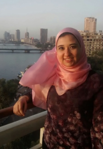
Jasmin Aghassi-Hagmann is a full professor at the Institute of Nanotechnology (INT) of the Karlsruhe Institute of Technology (KIT) in the Department of Electrical Engineering and Information Technology. She received her diploma in physics from RWTH Aachen and PhD from KIT, Karlsruhe. She has spent several years in R&D in the semiconductor industry (Infineon Technologies, IBM Semiconductor Alliance East Fishkill, Intel) developing advanced CMOS nodes. Her research interests are solution processible materials, 2D and 3D functional printing as well as thin film electronic devices and circuits. She serves in various national and international committees such as topic speaker in the Helmholtz Society Research Program Materials System Engineering, and is a member of the executive editorial boards of J-FPE and IEEE J-FLEX and others.
Webinar Description
Printed and flexible electronics enable interesting novel applications in the fields of sensors [1], bioelectronics [2], and security applications [3], to name but a few. Most of them gain their functionality from a layered structure composed of different materials that interact with each other. For semiconducting layers, organic and inorganic materials can be used; in this regard, the respective functional materials need to be formulated into inks that are then printed on various substrates. The structuring process of printing is a complex process in which many chemical and physical process parameters need to be controlled at the same time, such as drop volume, the waveform of the electrical signal controlling droplet formation, or the drying time. Also, the surface of the substrate plays a decisive role in printing accuracy and layer morphology. After printing, post-treatments are often necessary to obtain the desired features, since the properties of bulk materials often differ from printed nanoparticulate or precursor-derived layers.
This presentation starts by introducing various semiconducting inks based on either nanoparticle or precursor solutions and discusses thin film properties, microstructure, and finally the step-by-step device fabrication processes. Various printing techniques such as (super)-inkjet, laser printing and microplotting will be shown. These printed materials display advantages such as high carrier mobilities, transparency, stability in air, non-toxicity, and can be prepared mostly by using water or alcohol-based solvents. Finally, examples of hybrid sensor systems comprising printed and standard CMOS components will be elaborated on.
[1] Cadilha Marques, Gabriel, Dennis Weller, Ahmet Turan Erozan, Xiaowei Feng, Mehdi Tahoori, und Jasmin Aghassi‐Hagmann. „Progress Report on “From Printed Electrolyte‐Gated Metal‐Oxide Devices to Circuits”. Advanced Materials 31, Nr. 26 (Juni 2019): 1806483. https://doi.org/10.1002/adma.201806483.
[2] Mahsa K. Saghafi, Srivatsan K. Vasantham, Navid Hussain, George Mathew, Federico Colombo, Barbara Schamberger, Eric Pohl, Gabriel Cadilha Marques, Ben Breitung, Motomu Tanaka, Martin Bastmeyer, Christine Selhuber-Unkel, Ute Schepers, Michael Hirtz, Jasmin Aghassi-Hagmann, “Printed Electronic Devices and Systems for Interfacing with Single Cells up to Organoids”, Adv. Funct. Mat., Early View, 2023, https://doi.org/10.1002/adfm.202308613
[3] Zimmermann, Lukas, Alexander Scholz, Mehdi B. Tahoori, Jasmin Aghassi-Hagmann, und Axel Sikora. „Design and Evaluation of a Printed Analog-Based Differential Physical Unclonable Function“. IEEE Transactions on Very Large Scale Integration (VLSI) Systems 27, Nr. 11 (November 2019): 2498–2510. https://doi.org/10.1109/TVLSI.2019.2924081.
Webinar Agenda
- Introduction and greetings – 5 minutes
- Main talk – 55 to 60 minutes
- Q&A – 25 to 30 minutes
- The German Chapter of the IEEE Consumer Technology Society is pleased to announce a webinar by Prof. Tim Piessens, of MICAS, KU Leuven, that will take place on 18 December 2024 at 9.00 am, German time. All members of the German IEEE SSCS Chapter, as well as every other interested person, are heartily welcome to participate in this event.
Challenges in Battery Monitoring Systems for Electrical Vehicles
Date and Time:Wednesday, December 18, 2024
9:00 PM (German time)Register: https://lnkd.in/dCb-X2Zg
Description:Electrical vehicles will become the standard in private transport in the coming decade. Since the battery is still the main component that will determine cost and driving range, good battery control is the main component in an eV system. A battery management system consists of 2 components: a current measurement system and a voltage monitoring system. Both have their own specific problems. We will first discuss the different techniques to measure current: using a shunt, a Rogowski coil or a magnetic sensor. Next, the voltage measurement chain will be tackled including techniques for dealing with the high voltages of a battery pack.
Speaker Biography:
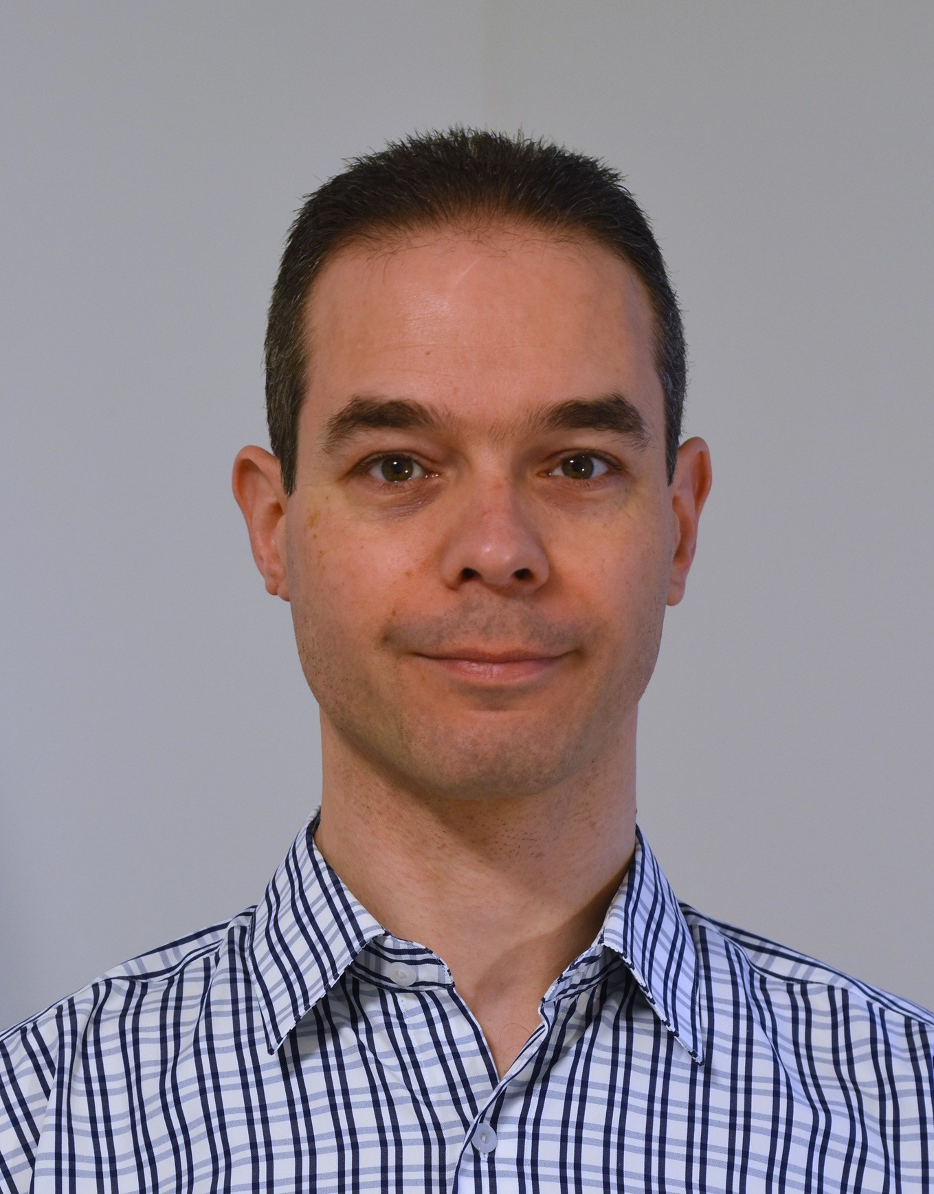
Tim Piessens received the M.Sc. and Ph.D. degrees in electrical engineering from the Katholieke Universiteit Leuven, Leuven, Belgium, in 1998 and 2003, respectively. During his Ph.D., he focused on a new type of power amplifier/line driver for xDSL applications. In 2004, he co-founded ICsense, where he is the CTO and is responsible for the technical content of projects in the medical, automotive and consumer fields. His current research interests include analog sensor readouts, non-linear system design, power management, high-voltage design and low-power, low-noise analog front-end design. From 2014 till 2021, he was a member of the IEEE International Solid-State Circuits Conference Technical Program Committee. He was a member of the ISSCC EU leadership, the ISSCC executive committee and the ISSCC vision committee from 2019 till 2021 and ITPC EU chair in 2021. From 2020 on, he is a member of the ESSDERC-ESSCIRC Steering Committee.Register: https://lnkd.in/dCb-X2Zg
Hosts:IEEE EGYPT Solid State Circuits Society Chapter
German Chapter of the IEEE Solid-State Circuits Society
IEEE Egypt CAS
-
Current and Future Trends of Solid State Devices
Date and Time
- Date: 22 Dec 2024
- Time: 06:00 PM to 07:30 PM
- All times are (UTC+01:00) Berlin
Location
- Virtual attendance.
Hosts
Registration
- Starts 22 November 2024 12:00 AM
- Ends 21 December 2024 05:00 PM
- All times are (UTC+01:00) Berlin
- No Admission Charge
- https://events.vtools.ieee.org/event/register/447448
Speaker
Description
Moore’s law is approaching its limits due to complications encountering scaling process regrading power dissipation and reaching scaling limits. New devices, architectures and techniques are essential to overcome these challenges and encounter the rapidly increasing demands of future technologies and applications that will continue to revolutionize how current devices work. In this talk, a brief insight about latest trends studied to advance the semiconductor and solid state devices and highlight on the roadmap drawn to meet the future needs.
Speaker Biography

Dr. Yasmine Elogail holds an Assistant Professor Position at the Nanotechnology and Nanoelectronics Engineering Program and member of National Technology Lab Project in the Center for Nanotechnology at Zewail City of Science and Technology in Egypt. She is currently the Vice Chair of the IEEE Egypt SIGHT Group. She specializes in semiconductor physics and engineering, cleanroom fabrication processes, simulation, modeling and characterization of solid state advanced devices. She worked as Scientific Researcher at the Institute of Semiconductor Engineering at University of Stuttgart in Germany, where she obtained her Ph.D. in Electrical Engineering.
-
How (and why) Si won the race toward millimeter-wave ICs
Date and Time
- Date:
12 January 20259 February 2025 - Time: 05:00 PM to 06:30 PM
- All times are (UTC+01:00) Berlin
Location
- Virtual attendance.
Hosts
Registration
- Starts 12 December 2024 12:00 AM
- Ends 9 February 2025 12:00 AM
- All times are (UTC+01:00) Berlin
- No Admission Charge
- https://events.vtools.ieee.org/event/register/452157
Speaker
- Dr.-Ing. Hermann Schumacher, Professor, Universität Ulm (retired)
Description
From Ka-band satellite applications to automotive radars at 77 GHz, systems in the upper microwave and millimeter-wave ranges are enabled by integrated circuits on Silicon wafers. And, judging from current publication activities, this trend will continue for the foreseeable future, and toward even higher frequencies, well into the THz range.When it comes to its physical properties, Si is an unlikely competitor for group III-V materials such as GaAs or InP. Lossy substrates and lower electron mobility, for instance. So why is it so successful? Cost is the easiest answer, but, unless we’re talking truly huge market sizes, GaAs ICs can be quite cost-competitive, area-wise.Silicon as a substrate for microwave circuits has been contemplated since at least 1965. Until the mid 1990s, Silicon monolithic microwave ICs (MMICs) tried to imitate GaAs, with limited success. The advent of Si/SiGe heterojunction bipolar transistors changed its approach drastically. The integrability of Si/SiGe HBTs into established bipolar and BiCMOS processes allows microwave and millimeter-wave chips with a high integration density, combined with digital functionality, and occasionally even micro-electro-mechanical structures.Using results from the literature as well as my own research, I will talk about the history of Si MMICs, some milestones, as well as current trends.Speaker Biography

Hermann Schumacher received his Diploma in Electrical Engineering in 1982, and his Doctorate in Engineering (Dr.-Ing., with highest distinction) in 1986, both from RWTH Aachen University. In 1986, he joined Bell Communications Research in Red Bank, NJ, USA, researching compound semiconductor devices for optoelectronic integration of high-speed fiberoptic applications. Among other things, he was involved in early work on InP/InGaAs heterojunction bipolar transistors (HBTs).In 1990, he joined Ulm University, Ulm, Germany. There, he and his research group worked on Si/SiGe HBTs (initially with the Daimler Research Center in Ulm), and, increasingly, microwave and millimeter-wave integrated circuits. From 2000 until 2016, he led the Competence Center on Integrated Circuits in Communications, a public-private partnership. Investigated applications ranged from short-range ultra-wideband radars for vital sign detection and security systems to complex frontend ICs for active electronically scanned satellite antennas.
From 2011 until 2022, Professor Schumacher developed and directed the School of Advanced Professional Studies, the continuing education unit of Ulm University.
In 2023, he retired from his positions at Ulm University, but is still actively pursuing his research interests, as well as teaching continuing education courses.
- Date:
-
ADC Innovations for Improved Resolution, Power and Form Factor
Date and Time
- Date: 23. March 2025
- Time: 05:00 PM to 06:30 PM
- All times are (UTC+01:00) Berlin
Location
- Virtual attendance.
Hosts
Registration
-
- Starts 25. Fabruary 2025 12:00 AM
- Ends 23. March 2025 04:00 PM
- All times are (UTC+01:00) Berlin
- No Admission Charge
- https://events.vtools.ieee.org/m/470864
Speaker
- Dr. Pieter Harpe, Associate Professor, Eindhoven University of Technology
Description
ADC design is progressing rapidly over time thanks to innovations in architecture, circuit implementation, and technology scaling. For many emerging applications, for instance in the field of IoT or medical devices, converters with high resolution, low power consumption, and a small form factor are desired. In this tutorial-level presentation, we will explain the general trade-offs for these performance metrics, and we will highlight some of the recent developments that pushed the state-of-the-art forward. The talk will also give some insight into the challenges when embedding converters in an overall system.Speaker Biography
- Pieter Harpe (SM’15) received the MSc and PhD degrees from the Eindhoven University of Technology, The Netherlands, in 2004 and 2010, respectively. In 2008, he started as researcher at Holst Centre / imec, The Netherlands, where he worked on ultra low-power wireless transceivers, with a focus on ADC research and design. In April 2011, he joined Eindhoven University of Technology where he is currently an Associate Professor and lead of the Resource Efficient Electronics Lab. His main activities are on low-power analog and mixed-signal circuits, for instance for biomedical applications, internet of things, and edge AI. Dr. Harpe is TPC member for ISSCC and A-SSCC, Associate Editor for TCAS-I, SSCS AdCom Member-at-Large and SSCS Distinguished Lecturer. He previously served as TPC member for ISSCC, TPC member and track chair for ESSCIRC/ESSERC and co-organizer for AACD, was an IEEE SSCS Distinguished Lecturer in 2016/2017, and is recipient of the ISSCC 2015 Distinguished Technical Paper Award .


