6th Symposium on Schottky Barrier MOS (SB-MOS) devices
The 6th Symposium on Schottky Barrier MOS (SB-MOS) deviceswas held on September 8, 2022at the Competence Center for Nanotechnology and Photonics atTHM – University of Applied Sciences. It was organized by the EDS Germany Chapter and co-sponsored by THM. It was attended by approx. 50 participants in hybrid.
After a short welcome of Prof. Kloes with a detailed schedule, the presentations started with Prof. Richard Forbes from University of Surrey (UK). Prof. Forbes referred on “Apparent conceptual oversight in the statistical mechanics of the reverse-biased Schottky junction, and equivalent devices” with fundamental physics on Schottky junctions. He reported what appears to be a fundamental oversight in the basic statistical mechanics of counting transfers of electrons across a boundary between different media. As physicist he encouraged scientists to be precise in their articles in wording on field emission, thermionic emission or more precise thermal emission, etc. This was acknowledged by the participants.
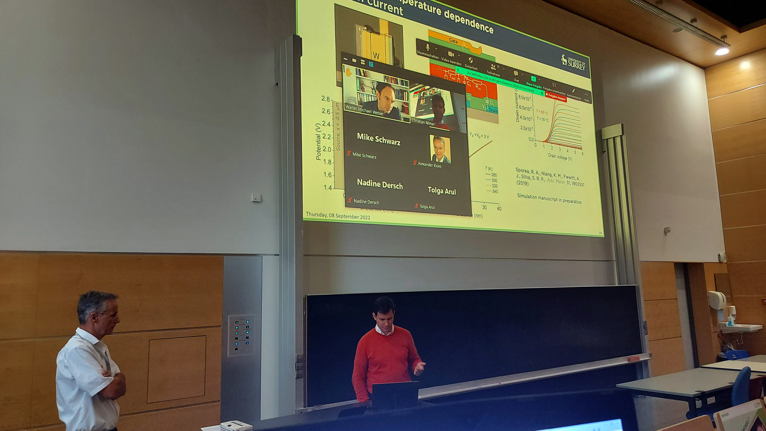
The next talk was given by Prof. Radu Sporea from University of Surreyon the topic “Contact-controlled TFT design addressing barrier-induced limitations”. He offered, that contact-controlled thin-film transistors are able to achieve superior gain,
low-voltage saturation and uniformity performance at the expense of switching speed
and current density. Prof. Sporea showed that conventional TFT-oriented optimization strategies require adaptation when the contact properties dominate causedfrom choices of constructive and operating parameters. He covered them systematically in this talk, alongside new insights into strategies for reducing temperature dependence. After the presentation a lot of discussions took place which allowed for a short coffee break. Discussions were continued during the break.
Prof. Radu Sporea during the discussion on his presentation.
Afterwards, “Prospects of SBMOS for cryogenic applications” by Prof. Laurie Calvet from CNRS (FR) gave very interesting insights of experimental devices based on superconducting Schottky barrier devices also well known as Josephson junctions. She explained the history and challenges and improvements of those junctions targeting quantum computing applications. The participants were very interested and also here a lot of discussion took place after the presentation.
The symposium continued with “SPICE compact modelling of amorphous oxide semiconductor memristive devices for memristive neural network” by Guilherme Carvalho fromUniversidade do Porto (P). The PhD candidate Carvalho presented experimentally fabricated Mo/a-IGZO/Ti/Mo memristors, in which we deposited the IGZO film by RF-magnetron co-sputtering from three binary ceramic targets and the capability of the device electrical characteristics. He fitted the devices with the Dynamic Memdiode Model (DMM) from Prof. Enrique Miranda’s group, which is well suited for the SPICE circuit simulation of hybrid CMOS-memristor circuits. Those results were benchmarked by simulating a single layer perceptron (SLP) circuit while classifying the handwritten images of the MNIST dataset, reaching an accuracy of ~90%.
The session was continued by the work of the PhD candidate Yiyi Yan from Université catholique de Louvain (BE) on the topic of “Hexagonal Boron NitrideMemristorBased on a NanogapSelf-Formed”.Ms. Yan offered detailed process comics of the different steps she applied to manufacture her devices. Those were supported by optical images (TEM, SEM) of important steps, e.g. Pt silicidation or the wet transfer of CVD-grownh-BN sheets. Impressive was the uniformity of the PtSi process as well as the impact of the various steps and changes onto the memristor device performance, which finally led to significant improvements.
After the lunch PhD candidate Christian Römer from THM – University of Applied Sciences (DE) gave some new insight in “Compact Modelling of Injection Current and Channel-Resistance Effects in Reconfigurable Field-Effect Transistors”. Römer showed the problem of describing the current-voltage characteristics of long channel Schottky barrier field-effect transistors. Here, the resistance of the channel must be considered in the characteristics. He showed a closed-form and physics-based compact model that combines a Schottky-barrier injection current with the limiting effect of a channel resistance. The model was compared with experimental data from NamLab and is in an excellent agreement to those.
Afterwards, Prof. Aníbal Pacheco-Sánchez from Universitat Autònoma de Barcelona (ES)continued on the topic of “Schottky barrier characterization of one-dimensional field-effect transistors”. He introduced into the topic and offered a new approach for 1D devices by the Landauer-Büttiker approach, which led him to a 1D LBM (Landauer-Büttiker Model). Prof. Pacheco-Sánchez compared the model with the 3D AEM and offered a lot of results for the extracted Schottky barrier heights. During the discussion afterwards, the experts agreed that this model is helpful by extracting the Schottky barrier height of 1D devices.
The last presentation of the Symposium was given by Prof. Walter Weber from TU Vienna (AT) and entitled “Exploring the novel Al – SixGe1-xSchottky FET system for the realizationof functionality enhanced transistors, optoelectronics and cryo-electronics”. He was referring on activities of the last decades on Silicon-Germanium and Aluminum material systems in microelectronics. Prof. Weber explained, by combining these materials in the form of geometrically confined nanowires and nanosheets new types of junction formation processes have been recently discovered. It has been found that pure Al-Si nanometer-scale system form atomically sharp Schottky, void-free and single crystal heterojunctions through a thermally driven material solid-state exchange reaction. The reliable Al-Si and Al – SixGe1-x nano-junctions have been found to be promising for the realization of runtime reconfigurable transistors (RFET) featuring electrically programmable n- and p-type polarity control due to their near midgap Fermi level pinning behavior. Pure Ge and Ge rich SixGe1-x channels functionality can be further increased to feature tunable negative differential resistance (NDR) that can be exploited for oscillators and enhanced photodetectors. In addition, the high purity of the single-crystal Al formed by exchanging the Ge and SixGe1-xlayers allows superconductivity below the critical temperature of 1.46 K and the observation of supercurrents in Ge providing a promising device platform for cryogenic electronics. As before, also here a lot of discussion took place.
Prof. Laurie Calvet closed the Symposium with some finally remarks, that Schottky barrier junctions offer a wide spectrum of applications.